Signal chain
Both channels do the same thing, end to end, with the same logic: a decoder, a FIFO chain, a 256 MiB DDR3 ring behind one shared memory controller, and a USB pipe. Channel 2 is a copy of channel 1 — same decoder parameters, same FIFO cores, same ring size — on its own input pin, its own half of DDR3 and its own endpoint.
Inputs
The board has a 200 MHz oscillator (sysClkp/sysClkn), doubled to a 400 MHz
genClk that clocks the decoders. Each channel takes one single-ended 3.3 V
Manchester line:
- Channel 1 on J2-2 → FPGA pin
Y6 - Channel 2 on J2-4 → FPGA pin
AA6
These two pins are a differential pair
Y6 and AA6 are B34_L18P and B34_L18N — the most tightly coupled
trace pair on the connector. Using them as two independent single-ended
inputs is legal, but expect crosstalk to be the first suspect if the two
channels interfere at high rates. At 8.33 MHz no crosstalk has been
observed.
Per channel
manchester ──▶ mandec ──▶ 1→4 bit FIFO ──▶ 4→32 bit FIFO ──▶ [ buffer ] ──▶ okBTPipeOut
                  │                                                              │
               dec_clk (recovered, stalls when idle)                       okClk (USB)
mandec recovers a clock from the data and emits one bit per recovered edge.
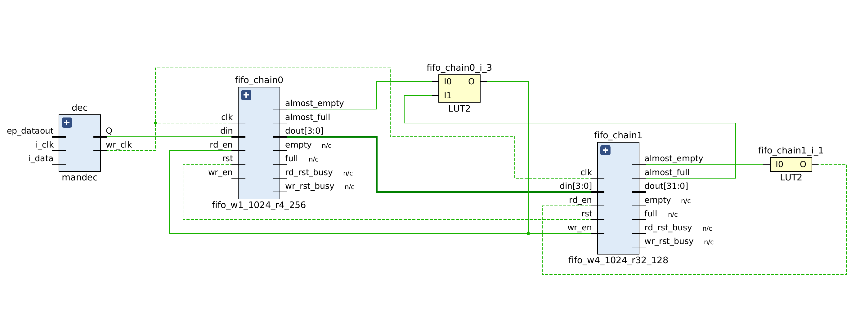
The FIFO chain widens that single bit to the 32-bit words the USB pipe moves.
See Manchester decoder for how the recovery works.
The buffer
Both channels take the same route into and out of DDR3:
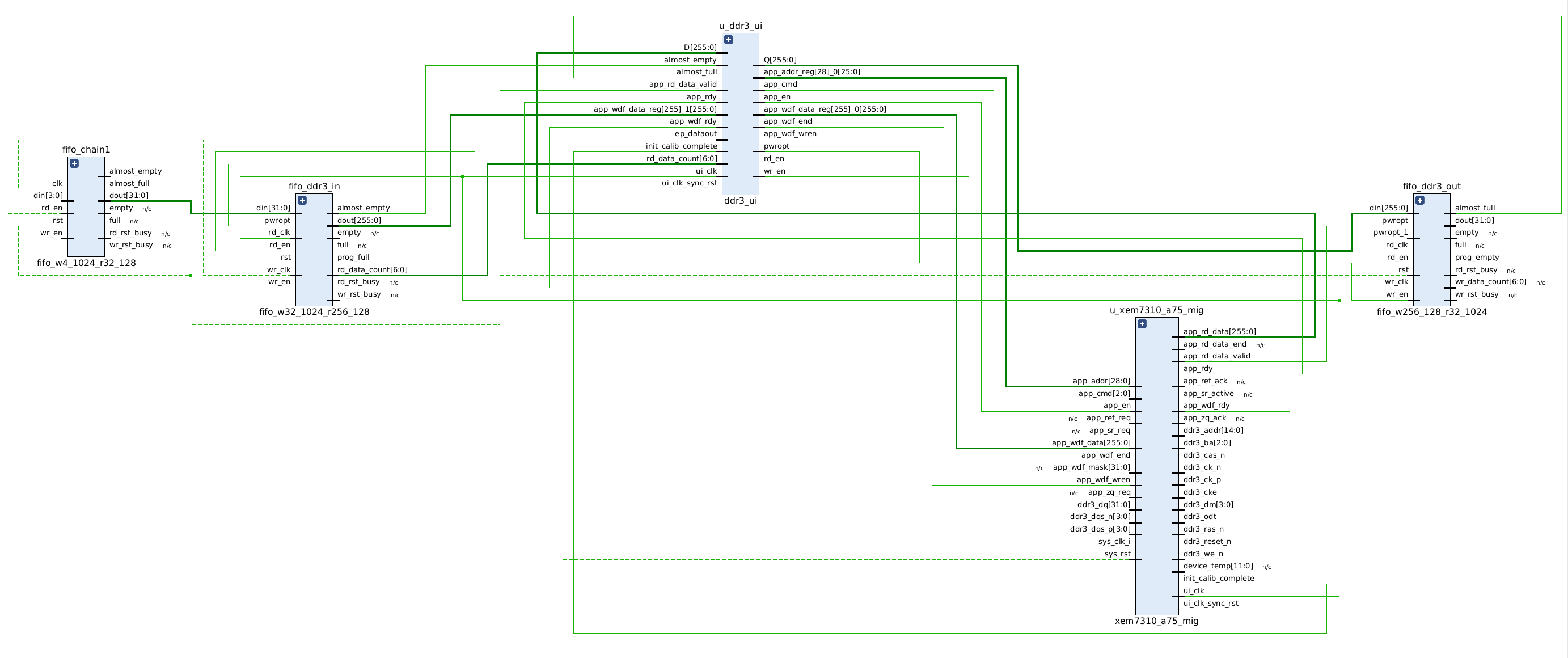
... ──▶ fifo*_ddr3_in ──▶ [ ddr3_ui ] ──▶ DDR3 (via MIG) ──▶ fifo*_ddr3_out ──▶ pipe
              │                │                                    │
        recovered clock     ui_clk                               ui_clk
Each channel gets a ring of its own — 256 MiB, roughly four minutes at 8.33 Mbit/s. That capacity is the point: a host stall has to last minutes, not milliseconds, before anything is lost.
One controller, so the rings are not the whole device
RING_ADDR_BITS = 26 in ddr3_ui.v sets 256 MiB per channel. The rings
deliberately stop short of the 1 GiB the board carries: a ring only has to
outlast a host stall, and leaving headroom means the address mapping does
not have to be exactly what the MIG documentation implies.
Sharing one memory controller
There is one MIG, so ddr3_ui time-shares its user interface between the two
channels. The rings sit in disjoint halves of the address space:
channel 1   app_addr [0 .. 2^26)
channel 2   app_addr [2^26 .. 2^27)
s_idle chooses between four jobs — read and write, per channel —
round-robin: it grants the first ready job at or after a rotating pointer,
then moves the pointer past it. There is no fixed priority, so neither channel
can starve the other however backlogged it gets.
Round-robin is load-bearing
With a fixed write-then-read priority, channel 1's writes and reads keep
the controller permanently busy and channel 2 never gets a burst.
tb_ddr3_ui shows it: revert the pointer update and channel 2 delivers
0 bursts in the time channel 1 delivers 200.
Bandwidth is not the constraint. Two channels at 8.33 Mbit/s need about 2 MB/s between them, which even this unpipelined state machine clears by more than two orders of magnitude.
Resetting the input side
Each channel's input side — fifo*_chain0/1 and fifo*_ddr3_in — runs on that
channel's recovered clock, which stops whenever its decoder sees no valid
symbols. Those FIFOs therefore take a sequenced reset instead of the host's
reset — see The FIFO reset sequencer.
Host interface
All Opal Kelly endpoints are OR'd into the okHost core:
| Endpoint | Direction | Purpose |
|---|---|---|
okWireIn 0x00 |
in | resets, see Pinout |
okBTPipeOut 0xA0 |
out | channel 1 data |
okBTPipeOut 0xA1 |
out | channel 2 data |
okWireOR is instantiated with N = 2 and channel 2's endpoint occupies
okEHx[129:65]. Both pipes use ep_ready = ~prog_empty with the same 16-word
threshold, so the same host code drives either.
Schematics
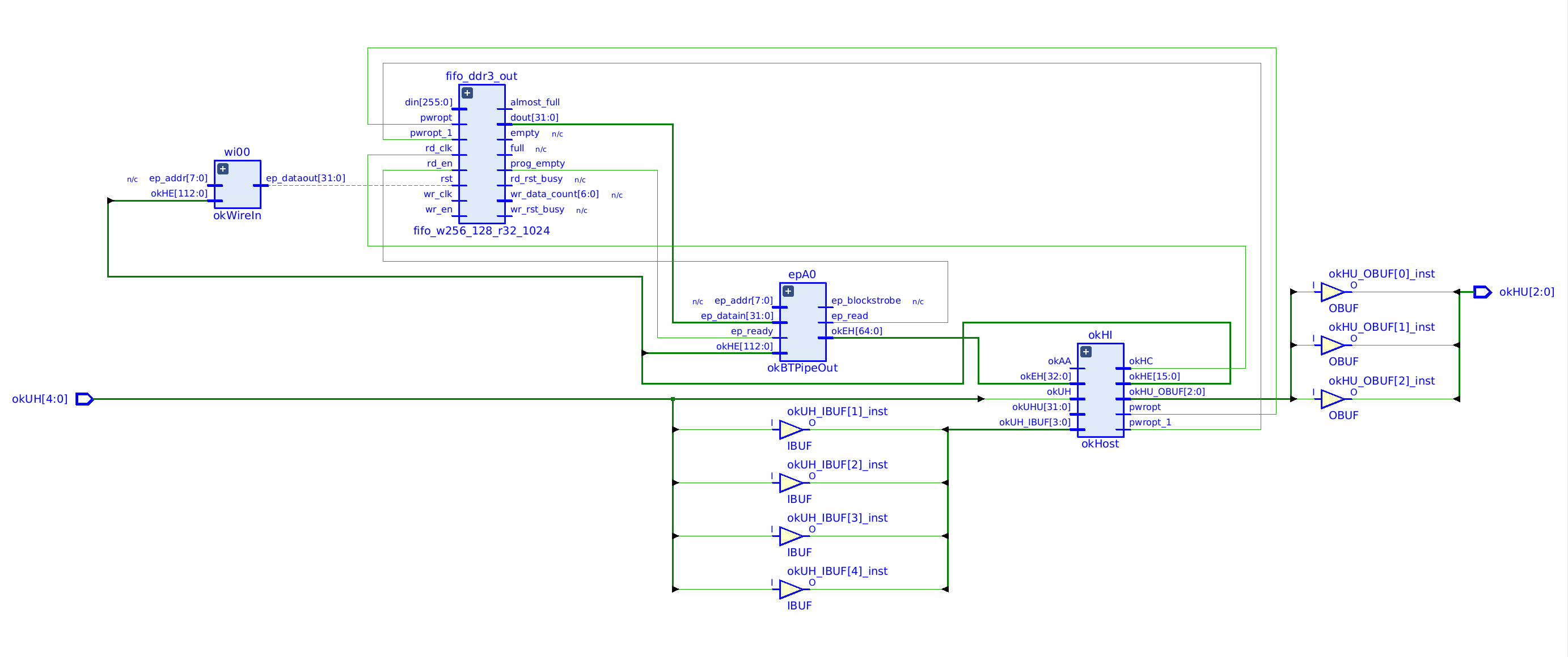
These schematics show one channel
They were exported from the single-channel design. The FIFO chain is the
same per channel. The DDR3 and host-side schematics are missing channel 2's
FIFOs, its ring and pipe 0xA1; the MIG side is unchanged.
The FIFO chain that widens one decoded bit into 32-bit words:
The DDR3 cache and its MIG user-interface logic:
The Opal Kelly host side: